As far back as 1965, Gordon Moore, the co-founder of the technology giant Intel, suggested that the number of transistors on a microchip doubles every two years.
But researchers have begun to question how long that doubling, which has since become known as Moore's Law, can continue. As processes become smaller - the current generation of microprocessors uses transistors just 32 nanometres (billionths of a metre) across - it becomes ever harder to make them even smaller. In short, there are limits, and they are not far off.
Busting through those limits could require a solution at the atomic level.
Some say the answer might lie in the quantum-mechanical process of "tunnelling", a phenomenon in which electrons are able to move through barriers.
Through the pull of a strong electric field, the outer electrons of an atom are able to escape from their binding nuclei, pushing particles through small walls to create a final ionised atom on the other side.
The aim is to develop a material that allows electrons to move more easily - and therefore allow energy to flow more efficiently through devices, providing smaller, faster, less power-hungry gadgets. Integrating such a material into device design is the focus of research being done at the Masdar Institute as the university prepares to install a cleanroom - a lab free of the dust that can fatally hinder work at the microscopic level of chipmaking.
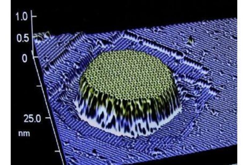
Researchers at Masdar are looking to germanium, which - mixed with silicon in the form of tiny crystals - can become embedded into memory devices to act as "stairs" on which electrons can travel.
In a delicate balance of memory retention, speed and power, these stairs allow excited electrons to be pushed through barriers within a data storage cell with about half as much power as usual.
A similar idea can be applied to solar-power films that alloy silicon with the lighter, cheaper, stronger germanium. Thin-film solar cells can be fitted to everything from rooftops and windows to the screens of smartphones, tablets and other gadgets.
One danger with electron transfer is leakage. A group at Masdar has been testing composites of germanium that, when layered in solar films and memory devices, minimise leakage.
Because germanium is far more expensive than silicon, researchers have been trying to grow thin germanium layers on cheaper substrates.
And for that, according to Ammar Nayfeh, the assistant professor of microsystems devices and circuits at Masdar Institute, the new cleanroom will be essential.
"The cleanroom will be the only one in the region where this material can be grown," he said.
Masdar students have already been gaining experience elsewhere. At the Massachusetts Institute of Technology's lab in the US, the microsystems engineering student Sabina Abdul Hadi was able to mix germanium with silicon in various proportions to create solar films of different thicknesses.
The 24 solar cells she made there are being tested at Masdar under a sun simulator to see what combination absorbs light best, yielding most energy. The goal is to find the combination that is best tuned to various wavelengths, so that electrons have enough energy to overcome gaps.
"As a solar cell is creating energy based on temperature or light, the amount of energy it leaks also depends on the material itself," she said.
"If you have a metal or an aluminium that is always charging, while a piece of cloth works as an insulator, the idea is to create something in between, that will charge but also insulate."
She is also testing different processes for chemically etching the surface of the film with microscopic pits that alter the way the light hits it. The methods involve dipping the samples into either liquid acid solution or concentrated chemical gases. Wet etching is faster, but gas is more precise.
"There are so many possibilities for getting the best results, and every single second is important for processing the material," she said.
Once perfected, the film will become "the next step of progression in solar cell research", Prof Nayfeh said.
"To really get beyond the challenges of solar cells and energy leakage, you have to take something standard and combine it with nanotechnology to create future devices," he said.
"The same applies to memory and increasing the output of the technology we use every day."
Others have been practising elsewhere. Ayman Rizk, a student of electronics and communications engineering, spent the summer at the National Nanotechnology Research Centre in Turkey developing "the next generation of the thumb drives we use in our daily lives".
Within the memory storage device, storage layers trap electrons, but often energy is lost as they travel through flooding gates within the drive.
These "floating" memories require a fairly thick oxide surrounding so that they can be charged with voltage to push and pull the electrons in and out of storage layers.
By instead storing electrons in tiny, thin-film particles, the electrons can travel easily while leakage is still contained. This also eliminates high-voltage charge bonds needed to push electrons through.
"This will need less power to push electrons through the isolator, achieving retention with less power, less time and high speed," Mr Rizk said.
"At the moment, flash drives are getting cheaper and have more capacity, but in the next five years there will be many limitations in how much energy we can trap. Nanocrystal memory is the best candidate for low power."
Mr Rizk is also testing eight samples of the crystals with different thicknesses and composition at Masdar Institute labs.
The technology would work not only for stand-alone memory used in mobile devices but also for technology being developed that would allow data-heavy computers to power down memories not currently being accessed, cutting down energy consumption.
"This could eventually be used for large projects, medical or advanced simulations," Prof Nayfeh said. "This is the future of computing."